Accelerate AI Applications on Xilinx VCK190 Evaluation Kit with Design Gateway's IP Cores
2022-11-18
Xilinx's Versal AI Core series devices are designed to solve the unique and most difficult problem of AI inference by using a high computation efficiency ASIC-class AI compute engine together with a flexible programmable fabric to build an AI application with accelerators that maximize efficiency for any given workload while delivering low power and low latency.
The Versal AI Core series VCK190 evaluation kit features the VC1902 device which has the best AI performance in the portfolio. The kit is made for designs requiring high-throughput AI inference and signal processing computing performance. Delivering 100 times greater computing power than current server-class CPUs and having various connectivity options makes the VCK190 kit an ideal evaluation and prototyping platform for a diverse range of applications from the cloud to the edge.
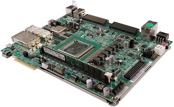 Figure 1: Xilinx Versal AI Core series VCK190 evaluation kit. (Image source: AMD, Inc)
Key features of the VCK190 evaluation kit
- Onboard Versal AI Core Series device
- Equipped with Versal ACAP XCVC1902 production silicon
- AI and DSP Engines providing 100X greater compute performance over today’s server-class CPUs
- Pre-built partner reference designs for rapid prototyping
- Latest Connectivity technology for leading edge application development
- Built-in PCIe® Gen4 Hard IP for high performance device interface such as NVMe SSD and Host Processors
- Built-in 100G EMAC Hard IP for high speed 100G network interfaces
- DDR4 and LPDDR4 memory interfaces
- Co-Optimized Tools and Debug Method
- Vivado® ML, Vitis™ unified software platform, Vitis AI, AI Engine tools for AI Inference application development
AI Interface Acceleration with Xilinx's Versal AI Core Series devices
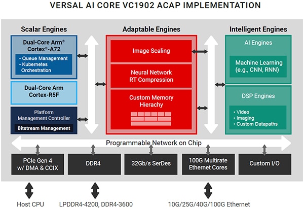 Figure 2: Xilinx Versal AI Core VC1902 ACAP device block diagram. (Image source: AMD, Inc)
The Versal® AI Core adaptive compute acceleration platform (ACAP) is a highly integrated, multicore, heterogeneous device that can dynamically adapt at the hardware and software level for a wide range of AI workloads, making it ideal for AI edge computing applications or cloud accelerator cards. The platform integrates next-generation Scalar Engines for embedded compute, Adaptable Engines for hardware flexibility, and Intelligent Engines consisting of DSP Engines and revolutionary AI Engines for inference and signal processing. The result is an adaptable accelerator that exceeds the performance, latency, and power efficiency of traditional FPGAs and GPUs for AI/ML workloads.
Versal ACAP Platform highlight
- Adaptable Engines:
- Custom memory hierarchy optimizes data movement and management for accelerator kernels
- Pre- and post-processing functions including neural network RT compression and image scaling
- AI Engines (DPU)
- Tiled array of vector processors, up to 133 INT8 TOPS performance with XCVC1902 devices, called, Deep Learning Processing Unit or DPU
- Ideal for neural networks ranging from CNN, RNN, and MLP; hardware adaptable to optimize for evolving algorithms
- Scalar Engines
- Quad-Core ARM processing subsystem, Platform management controller for security, power and bitstream management
VCK190 AI Inference performance
VCK190 is capable of delivering over 100X greater compute performance compared to current server class CPUs. Below is an example of performance based on AI Engine implementation by C32B6 DPU Core with batch = 6. Refer to the following table for the throughput performance (in frames/sec or fps) for various neural network samples on VCK190 with the DPU running at 1250 MHz.
|
Table 1: Example of VCK190 AI Inference performance.
See more detail of VCK190 AI performance from Vitis AI Library User Guide (UG1354), r2.5.0 at https://docs.xilinx.com/r/en-US/ug1354-xilinx-ai-sdk/VCK190-Evaluation-Board
How Design Gateway's IP cores accelerate AI application performance?
Design Gateway's IP Cores are designed to handle Networking and Data Storage protocol without need for CPU intervention. This makes it ideal to fully offload CPU systems from complicated protocol processing and which enables them to utilize most of their computing power for AI applications including AI inference, pre and post data processing, user interface, network communication and data storage access for the best possible performance.
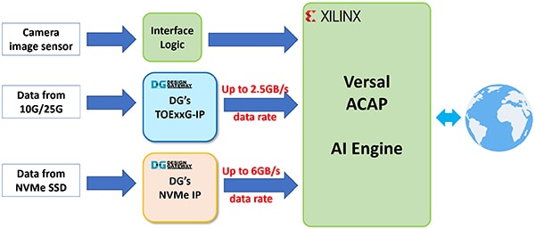 Figure 3: Block diagram of example an AI Application with Design Gateway's IP Cores. (Image source: Design Gateway)
Design Gateway's TCP Offload Engine IP (TOExxG-IP) performance
Processing high speed, high throughput TCP data streams over 10GbE or 25GbE by traditional CPU systems needs more than 50% of CPU time which reduces overall performance of AI applications. According to 10G TCP performance test on Xilinx's MPSoC Linux systems, CPU usage during 10GbE TCP transmission is more than 50%, TCP send and receive data transfer speed could be achieved just around 40% to 60% of 10GbE speed or 400 MB/s to 600 MB/s.
By implementing Design Gateway's TOExxG-IP Core, CPU usage for TCP transmission over 10GbE and 25GbE can be reduced to almost 0% while ethernet bandwidth utilization can be achieved close to 100%. This allows the sending and receiving of data over the TCP network directly by pure hardware logic and be fed into the Versal AI Engine with minimum CPU usage and the lowest possible latency. Figure 4 below shows the CPU usage and TCP transmission speed comparison between TOExxG-IP and MPSoC Linux systems.
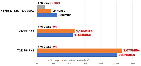 Figure 4: Performance comparison of 10G/25G TCP transmission by MPSoC Linux systems and Design Gateway's TOExxG-IP Core. (Image source: Design Gateway)
Design Gateway’s TOExxG-IP for Versal devices
 Figure 5: TOExxG-IP systems overview. (Image source: Design Gateway)
The TOExxG-IP core implements the TCP/IP stack (in hardwire logic) and connects with Xilinx’s EMAC Hard IP and Ethernet Subsystem module for the lower-layer hardware interface with 10G/25G/100G Ethernet speed. The user interface of the TOExxG-IP consists of a Register interface for control signals and a FIFO interface for data signals. The TOExxG-IP is designed to connect with Xilinx's Ethernet subsystem through the AXI4-ST interface. The clock frequency of the user interface depends on the Ethernet interface speed (e.g., 156.625 MHz or 322.266 MHz).
TOExxG-IP’s features
- Full TCP/IP stack implementation without need of the CPU
- Supports one session with one TOExxG-IP
- Multi-session can be implemented by using multiple TOExxG-IP instances
- Support for both Server and Client mode (Passive/Active open and close)
- Supports Jumbo frame
- Simple data interface by standard FIFO interface
- Simple control interface by single port RAM interface
FPGA resource usages on the XCVC1902-VSVA2197-2MP-ES FPGA device are shown in Table 2 below.
|
Table 2: Example Implementation Statistics for Versal device.
More details of the TOExxG-IP are described in its datasheet which can be downloaded from Design Gateway’s website at the following links:
Design Gateway's NVMe Host Controller IP performance
NVMe Storage interface speed with PCIe Gen3 x4 or PCIe Gen4 x4 has data rates up to 32 Gbps and 64 Gbps. This is three to six times higher than 10GbE Ethernet speed. Processing complicated NVMe storage protocol by the CPU to achieve the highest possible disk access speed requires more CPU time than TCP protocol over 10GbE.
Design Gateway solved this problem by developing the NVMe IP core that is able to run as a standalone NVMe host controller, able to communicate with an NVMe SSD directly without the CPU. This enables a high efficiency and performance of the NVMe PCIe Gen3 and Gen4 SSD access, which simplifies the user interface and standard features for ease of usage without needing knowledge of the NVMe protocol. NVMe PCIe Gen4 SSD performance can achieve up to a 6 GB/s transfer speed with NVMe IP as shown in Figure 6.
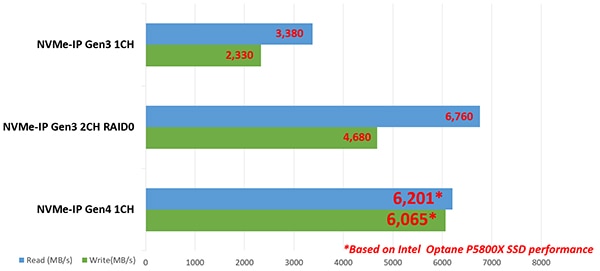 Figure 6: Performance comparison of NVMe PCIe Gen3 and Gen4 SSD with Design Gateway's NVMe-IP Core. (Image source: Design Gateway)
Design Gateway's NVMe-IP’s for Versal devices
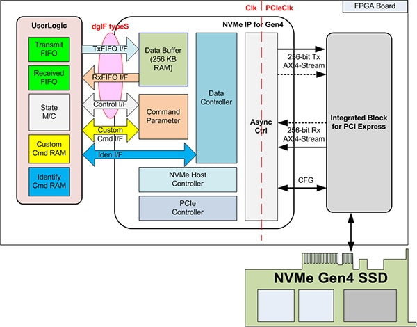 Figure 7: NVMe-IP systems overview. (Image source: Design Gateway)
NVMe-IP’s features
- Able to implement application layer, transaction layer, data link layer, and some parts of the physical layer to access the NVMe SSD without a CPU or external DDR memory
- Operates with Xilinx PCIe Gen3 and Gen4 Hard IP
- The ability to utilize BRAM and URAM as data buffers without needing an external memory interface
- Supports six commands: Identify, Shutdown, Write, Read, SMART, and Flush (optional additional command support available)
FPGA resource usages on the XCVC1902-VSVA2197-2MP-E-S FPGA device are shown in Table 3.
|
Table 3: Example Implementation Statistics for Versal device.
More details of the NVMe-IP for Versal device are described in its datasheet which can be downloaded from Design Gateway’s website at the link below:
NVMe IP Core for Gen4 Xilinx Datasheet
Conclusion
Both the TOExxG-IP and NVMe-IP core could help accelerate AI application performance by fully offloading CPU systems from compute and memory intensive protocol such as TCP and NVMe Storage protocol which is critical for real-time AI application. This allows Xilinx's Versal AI Core series device to to perform AI inference and high-performance computing applications without bottleneck or delay from network and data storage protocol processing.
The VCK190 evaluation kit and Design Gateway’s network and storage IP solution enable the best possible performance in AI applications with the lowest possible FPGA resource usage and very high power efficiency on Xilinx's Versal AI Core device.
Disclaimer: The opinions, beliefs, and viewpoints expressed by the various authors and/or forum participants on this website do not necessarily reflect the opinions, beliefs, and viewpoints of DigiKey or official policies of DigiKey.


